High Efficiency Wide Load Range Buck_Boost_Bridge Photovoltaic Microconverter
Date:2019-04-28 23:52:27 Posted by:louis.xi View:502
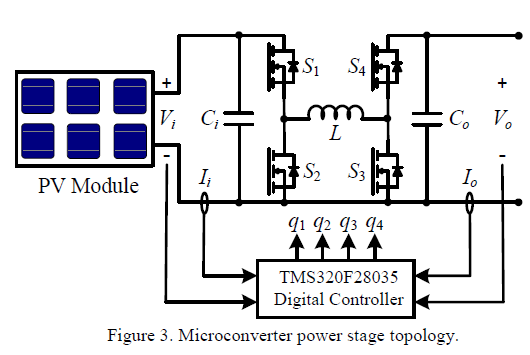
The power stage, illustrated in Fig. 3, comprises buckside
switches, S1-S2, boost-side switches, S3-S4, an inductor,
L, and input and output capacitors, Ci and Co, respectively. In
addition, there are low-side current sensing resistors and
buffer amplifiers to enable the acquisition of input and
output voltage and current as well as 5V and 12V on-board
house-keeping supplies powered by the PV source.
The power stage is intended to be compatible with a wide
variety of PV sources and a string inverter loads. In addition,
it is expected to harvest energy from partially-shaded PV
sources. To accomplish these goals, the topology must
operate in buck mode or boost mode.
The power stage is designed to operate at a nominal input
maximum power point (MPP) of about 40 V and 5 A (IM,
VM). The inductance is 40 μH. At the MPP, continuous
current mode (CCM) buck operation is guaranteed when the
input current exceeds approximately 300 mA for any buck
load current. Similarly, in boost mode, CCM is guaranteed
when the input current exceeds 2 A.
PWM constraints are imposed by minimum switch ONtimes
of 100 nsec (S2 and S4) and 133 nsec (S1 and S3) and a
dead time of 150 nsec at all switch transitions. Consequently,
the buck duty cycle, Dbu (the fraction of S1 ON-time) cannot
have a value between 0.9 and 1.0. Likewise, the boost duty
cycle, Dbo (the fraction of S3 ON-time) cannot exist between
0 and 0.033. The PWM method described below provides a
smooth transition between the buck and boost modes as load
current increases while adhering to all switching constraints.
The ideal dc gain of the converter is given by
 . (1)
. (1)
Buck mode switching, where Dbo = 0, is used for 0<G≤0.9,
where the minimum S2 ON-time is required. Likewise, boost
mode switching, where Dbu = 1, is used for G>1.034. The
duty cycle resolution is 0.00375% (150 psec steps).
To obtain similar resolution in the buck-to-boost
transition range, 0.9 < G < 1.034, bridge switching is
employed. The bridge mode is divided into two regions,
br_A and br_B, as shown in Fig. 4, where Dbu and Dbo are
plotted as a function of converter gain. At the low-gain end
of br_A, S3 is switched on for its minimum allowable time,
133 nsec, corresponding to Dbo = 0.033. At the same time,
Dbu = 0.875, which results in a gain of 0.9052. To increase
the gain within the br_A region, Dbu is increased up to a
maximum of 0.9 (again limited by S2 minimum ON-time),
corresponding to a converter gain of 0.9310. In the br_B
region, Dbo is varied while holding Dbu = 0.9. The high-gain
end of br_B, 1.033, is reached when a smooth transition to
boost mode can be made employing the minimum S3 ONtime.
It is worth noting that, given the minimum and dead
time switching constraints, this strategy achieves the
minimum possible average inductor current at all values of
gain and therefore minimizes the conductive losses in the
inductor and the switches.


Login
Enter your email address and password
© COOWA © 2018 Copyright